PCB 임베디드 저항 소자
Embedding Resistor Elements for PCB, Part 1
Designers Notebook by Vern Solberg, Consultant
내장형 저항기 기술이 수십 년의 역사에도 불구하고 "새롭고" "성장하는" 것으로 간주되는 이유는 무엇입니까? 사실, 기존의 수많은 PCB 제조업체는 저항 요소를 내장하는 재질과 프로세스에 대해 잘 알고 있지만 모두가 기존의 다층 회로 기판 고객 기반을 위해 설정된 절차를 변경할 준비가 되어있는 것은 아닙니다. 다음 질문은 "저항을 내장한 동기는 무엇입니까?" 입니다.
• PCB 고밀도화 - 주요 드라이버
• 기능 - 기여자
• 성능 - 향상된 기능
• PCB 어셈블리 - 단순화
Why is embedded resistor technology considered to be “new” and “growing” despite decades of history? In fact, a broad number of established PCB fabricators are knowledgeable about the materials and processes for embedding resistor elements but not all may be prepared to alter procedures established for their more conventional multilayer circuit board customer base. The next question is, “What is the motivation for embedding resistors?”
• PCB densification—a primary driver
• Functionality—a contributor
• Performance—an enhancement
• PCB assembly—simplified

다층 PCB의 레이어 내에 저항 요소를 내장 할 때의 주요 이점은 회로 기판 표면의 외부 표면에 배치된 주요 활성 구성 요소를 보다 효율적으로 배열하고 상호 연결할 수 있다는 것입니다. 또한 대부분의 수동 부품을 내장하면 극한 환경이나 최종 제품이 과도한 진동 및 충격에 노출 될 때 물리적으로 영향을 받지 않는 보다 견고한 PCB 어셈블리 개발에 기여할 수 있습니다. 또한 회로 기판 구조 내에 이러한 수동 저항 요소를 통합하면 손상되기 쉬운 세라믹 기반 부품의 조달, 재고 및 조립 처리에 필요한 물류가 간소화 됩니다.
The primary benefit of embedding resistor elements within the layers of the multilayer PCB is the ability to more efficiently arrange and interconnect the primary active components placed on the outer surface of the circuit boards surface. Furthermore, embedding most of the passive components can contribute to the development of a more robust PCB assembly, one that will not be physically impacted by environmental extremes or when the end product is exposed to excessive vibration and shock. Additionally, incorporating these passive resistor elements within the circuit board structure simplifies the logistics required for procurement, stocking, and assembly processing for multitudes of damage-prone ceramic based components.

PCB 설계자가 직면한 주요 문제는 회로 기판의 구조 내에 삽입하는데 더 적합한 저항과 회로 기판의 외부 표면에 배치하는데 더 적합한 저항 소자를 결정하는 것입니다. 인쇄 기판 설계자는 실제로 촉진자 역할을 하며 구성 요소를 포함하는 유일한 의사 결정자가 아닙니다.
인쇄 회로 기판에 대한 잠재적인 비용 영향으로 인해 저항을 내장하기로 결정하는 것은 엔지니어링 및 관리 수준의 문제일 가능성이 더 높습니다. 일반적으로 수동 부품을 장착하기 위해 예약된 제한된 표면적 및/또는 완성된 부품의 성능 향상 가능성으로 인해 정당화됩니다.
A key issue facing the PCB designer is to determine which resistors will be more suitable for embedding within the circuit board’s structure and which resistor elements are more appropriate for placement onto the circuit board’s outer surface. The printed board designer really acts as the facilitator and is rarely the sole decision maker for embedding components. Because of the potential cost impact on the printed circuit board, the decision to embed resistors is more likely an engineering and management level issue, typically justified by the restricted surface area reserved for mounting passive components and/or the potential for enhanced performance of the finished product.
임베디드 저항기 기술을 구현하기 위한 준비 과정에서 설계자 및/또는 프로그램 관리자는 먼저 기술 및 예산 (비용) 목표를 모두 충족하는 프로세스 (후막 또는 박막)를 선택하는 데 실질적인 지침을 제공 할 수 있는 숙련된 공급 업체를 찾아야합니다. 최종 제품을 위해 설립되었습니다. 형성된 저항기 요소는 인쇄된 후막 조성물 또는 이미지화되고 화학적으로 에칭된 박막 공정으로 제공 될 수 있습니다.
• 후막 저항기 재질은 광범위한 기본 값을 제공하기 위해 공식화 되었으며 광범위한 상업적 응용 분야에 성공적으로 사용되었습니다. 저항기 공식은 스크린 인쇄 또는 증착이 지정된 회로 기판 레이어에 제공된 사전 패터닝된 종단 랜드에 직접 요소를 형성 할 수 있도록 하는 탄소 충전 폴리머 화학을 기반으로 합니다.
• 박막 저항기는 저항성 재질로 미리 코팅된 동박 재질을 사용하여 형성됩니다. 레지스트 층은 전체 시트에 걸쳐 저항기 기본 값의 균일 성을 제공하는 증기 배치를 사용하여 구리 시트 재질 위에 증착됩니다.
In preparation for implementing embedded resistor technology the designer and/or program manager must first seek an experienced supplier company that can furnish practical guidance in selecting a process (thick-film or thin-film) that will meet both technical and budgetary (cost) goals established for the end product. Formed resistor elements may be furnished as a printed thick-film composition or an imaged and chemically etched thin-film process.
• Thick-film resistor materials are formulated to furnish a wide range of primary values and have been successfully used for a broad number of commercial applications. The resistor formulations are based on carbon-filled polymer chemistry that enables screen printing or deposition to form elements directly onto pre-patterned termination lands furnished on a designated circuit board layer.
• Thin-film resistors are formed using copper foil material that is pre-coated with resistive material. The resist layer is deposited onto the copper sheet material using vapor disposition that provides uniformity of the resistor base value across the entire sheet.
박막 저항기 재질은 Grade 3 동박을 사용하여 다양한 기본 값으로 제공됩니다. 박막 저항기 형성 공정을 위해 개발된 구리 시트는 18µm (0.5oz) 및 35µm (1oz) 두께로 제공됩니다. 이 시리즈의 이 기사에서 제공되는 정보는 "후막" 저항기 내장을 고려하는 회로 기판 설계 전문가에게 지침을 제공하기 위해 준비되었습니다. 임베딩을 위한 후보 저항을 식별 할 때 설계자는 저항 값 범위, 허용 오차 대역폭 및 애플리케이션을 모두 고려해야합니다.
Thin-film resistor materials are supplied in a variety of base values using Grade 3 copper foil. The copper sheets developed for the thin-film resistor forming process are available in thicknesses of 18 µm (0.5 oz) and 35 µm (1 oz). The information furnished in this installment of this series has been prepared to provide guidance to the circuit board design professional considering the implementation for embedding “thick-film” resistors. When identifying candidate resistors for embedding, the designer must consider both resistor value range, the allowable tolerance bandwidth, and application.
후막 저항기 형성 공정은 일반적으로 허용 오차가 덜 중요한 경우에 사용되며, 주로 종단 저항, 전류 제한, 트랜지스터 바이어스 및 정확한 값 허용 오차가 중요하지 않은 풀업/풀다운 저항을 위한 디지털 및 아날로그 회로 애플리케이션에 사용됩니다. . 저항기 기능 종단 저항기는 전기 전송선의 끝에 또는 차동 쌍 신호로 작업할 때 배치됩니다. 반면에 풀업 및 풀다운 저항은 논리 회로 애플리케이션에서 일반적으로 사용됩니다. 예를 들어 풀다운 저항의 기능은 다른 활성 장치가 연결되어 있지 않을 때 논리 신호를 0V에 가깝게 유지하는 것입니다. 풀업 저항의 기능은 전원과 접지 사이의 전압이 직접 연결되지 않도록 하는 것입니다. 회로 로직 유형에 따라 터미네이션, 풀업 및 풀다운 저항에 대해 선택한 일반적인 값은 500ohms에서 10Kohms 범위의 값으로 달라질 수 있으며 최대 ±20%의 허용 오차 한계를 허용 할 수 있습니다. "전류 제한"으로 지정된 저항 요소는 구성 요소를 통해 흐르는 전류 양의 상한을 설정하는데 사용되며 "트랜지스터 바이어스"저항은 일반적으로 트랜지스터 및 반도체 구성 요소와 함께 사용됩니다.
The thick-film resistor forming process is generally employed where tolerances are less critical, primarily used in digital and analog circuit applications for terminating resistors, current limiting, transistor biasing as well as for pull-up/pulldown resistors where precise value tolerances are not critical. Resistor Functionality Termination resistors are placed at the end of an electrical transmission line or when working with differential pair signals. Pull-up and pull-down resistors on, the other hand, are commonly used in logic circuit applications. For example, the function of the pull-down resistor is to hold the logic signal near to zero volts when no other active device is connected. The pull-up resistor’s function is to ensure that the voltage between power and ground cannot be directly connected. Depending on the circuit logic type, typical values selected for termination, pull-up and pull-down resistors can vary in values that range from 500 ohms to 10K ohms and may tolerate value tolerance limits as high as ±20%. Resistor elements designated for “current limiting” are used for setting an upper limit to the amount of current that flows through a component while “transistor biasing” resistors are commonly used in combination with transistors and semiconductor components.
후막 저항기 재질의 전반적인 성능은 최적화된 회로 설계 및 제조 프로세스와 관련이 있습니다. 회로 설계의 성능 요구 사항을 성공적으로 달성하려면 폴리머 후막 저항기의 재질 및 공정 매개 변수를 고려해야 합니다. 예를 들어, 특정 저항 요소에 사용할 랜드 크기 대 종횡비에 대한 결정은 여러 요인에 따라 달라집니다. 여기에는 목표 저항 값, 전기적 고려 사항, 사용 가능한 저항 값, 트리밍 요구 사항 및 동일한 보드 층에 있는 모든 저항의 저항 분포가 포함됩니다.
The overall performance of the thick film resistor materials is related to the optimized circuit design and fabrication process. The materials and process parameters of polymer thick-film resistor must be considered in order to successfully achieve the performance requirements of circuit designs. For example, the decision on what land size-to-aspect-ratio to use for a particular resistor element depends on a number of factors. These include target resistance values, electrical considerations, available resistivity values, trimming requirements, and the distribution of resistances of all the resistors present on the same layer of the board.

Table 1: Typical percentage distribution by resistor value.
일반적으로 대부분의 인쇄 회로 기판 설계에서 저항 값 분포는 로우 엔드에서는 1W에서 가장 높은 곳에서는 10MW로 다양합니다. 후막 저항을 위한 가장 실용적인 구성을 선택하는 PCB 설계자는 가장 눈에 띄는 기본 값 사용을 고려하고 값 범위의 하단을 용이하게 하는 재질을 선택해야 합니다. 통계적 관점에서 볼 때 디지털 또는 아날로그 회로에서 더 많은 수의 저항은 10W에서 10KW 사이의 범위에 속할 가능성이 높습니다 (표 1). 이를 염두에 두고 10W 재질을 기본 값으로 선택하면 광범위한 완성된 저항 값을 수용 할 수 있도록 저항 기하 구조를 확장하는 데 더 큰 유연성을 제공합니다. 지오메트리 원리 저항 재질의 지오메트리는 정사각형이나 직사각형처럼 간단할 수도 있고, 더 복잡한 저항 값의 경우 면적을 최소화하면서 저항 소자 길이를 최대화하도록 설계된 구불구불한 모양일 수 있습니다.
In general, on most printed circuit board designs, resistor value distribution will vary between 1W at the low end and 10MW at the highest. Selecting the most practical composition for the thick-film resistors, the PCB designer should consider the most prominent base-value usage and select a material that facilitates the lower end of the value range. From a statistical standpoint, the greater number of resistors in a digital or analog circuit will likely fall into a range between 10W and 10KW (Table 1). With that in mind, selecting the 10W material as the base value will provide greater flexibility in expanding the resistor geometry to accommodate a wide range of finished resister values. Geometry Principles The geometry of the resistance material can be as simple as a square or rectangle, or for more complicated resistor values, a serpentine shape designed to maximize resistor element length while minimizing area.
제공된 값은 사각형의 반대쪽 가장자리 사이에서 측정된 저항을 기반으로 합니다. 예를 들어, 두 개의 구리 랜드 사이에 인쇄되거나 증착된 1K 재질의 단일 사각형은 1K 저항 요소를 제공하는 반면 길이의 두 배 또는 두 개의 사각형 패턴은 2K 저항을 제공합니다. 직사각형 "바"형상 (그림 1)은 선택한 기본 후막 구성에 가까운 값을 가진 저항기에 가장 일반적이며, 저항 값이 후막 재질 기본 값보다 훨씬 클 때 서펜틴 형상이 사용됩니다.
The values provided are based on the resistance measured between opposite edges of a square. For example, a single square of 1K material printed or deposited between two copper lands will provide a 1K resistor element while a pattern that is twice the length, or two squares, furnishes a 2K resistor. The rectangular “bar” geometry (Figure 1) is most common for resistors with values close to the basic thick film composition selected while the serpentine geometry is employed when resistor values are significantly greater than the thick film materials base value.

Figure 1: Thick film resistor pattern variations.
"top-hat"모양의 저항기 형상은 일반적으로 목표 값에 도달하기 위해 광범위한 레이저 트리밍이 필요한 요소에 적용됩니다. 공급 업체는 설계자가 0.25mm (0.010 인치)보다 큰 저항 폭과 길이를 제공할 것을 권장합니다. 저항기 치수가 클수록 인쇄 변화에 대한 의존도 또는 구리 에칭 공정의 정확성이 줄어 듭니다.
The “top-hat” shaped resistor geometry is commonly applied for elements that will likely require extensive laser trimming to reach their target value. Suppliers recommend that designers furnish resistor widths and lengths greater than 0.25 mm (0.010 in). Larger resistor dimensions will reduce the reliance on the print variations or accuracy of the copper etching processes.
저항기 요소의 종단과 관련하여 저항기 종단에 제공된 랜드 패턴 형상은 후막 레지스트 재질의 공칭 0.25–0.50 mm 중첩을 허용하고 인쇄 프로세스 변수에 대한 허용치를 고려해야 합니다. 언급했듯이 후막 저항기 잉크 공식은 탄소 충전 폴리머 화학을 기반으로 합니다. 폴리머 매질 내 탄소 함량의 비율을 조정하여 재질을 공식화하여 광범위한 기본 값을 제공 할 수 있습니다. 레지스트 화합물의 인쇄 또는 증착 후 회로 기판은 150–250°C 범위의 온도에서 경화를 위해 오븐으로 전송됩니다. 인쇄 가능하거나 증착된 후막 저항 재질에 대한 5개의 상업적 소스와 이들이 제공하는 기본 값 범위가 표 2에 나와 있습니다. 응용 프로그램에 표 2에 명시된 것보다 더 나은 값 수정 또는 허용 오차가 필요한 경우 레이저 트리밍 시스템은 다음을 수행 할 수 있습니다. 필요한 조정을 위해 고용됩니다.
Regarding terminating the resistor elements, the land pattern geometry provided for the resistor termination should allow for a nominal 0.25–0.50 mm overlap of the thick-film resist material and consider allowances for printing process variables. As noted, the thick-film resistor ink formulations are based on a carbon-filled polymer chemistry. By adjusting the ratio of carbon content within the polymer medium, the material can be formulated to furnish a wide range of primary values. Following printing or deposition of the resist compound the circuit boards are transferred to an oven for curing at temperatures in a range between 150–250°C. Five commercial sources for printable or deposited thick-film resistive materials and the base value range that they offer are furnished in Table 2. When the application requires a value modification or a tolerance that is better than that noted in Table 2, laser trimming systems can be employed to make the necessary adjustments.

표 2: 두꺼운 필름 재료 선택 가이드. 참고: 5열에 표시된 저항 값 허용 오차는 인쇄 및 경화된 저항 재질을 나타냅니다.
Table 2: Thick film material selection guide. Note: The resistor value tolerance shown in column five represents the resistive material as printed and cured.
그림 2에 표시된 예는 특정 값 또는 허용 오차 목표를 달성하기 위해 레이저 기술을 사용하여 수정된 후막 저항기를 보여줍니다. 대량 PCB 제조를 위해 개발된 레이저 트리밍 시스템에는 기판 또는 다중 장치 패널 내의 모든 구성 요소 위치, 크기, 방향 및 레이아웃에 도달하도록 사전 프로그래밍된 다중 플라잉 프로브 접촉기가 장착되어 있습니다.
The examples shown in Figure 2 illustrate thick film resistors that have been modified using laser technology to achieve a specific value or tolerance target. Laser trimming systems developed for high volume PCB fabrication are equipped with multiple flying probe contactors that are preprogrammed to reach any component location, size, orientation and layout within the board or multi-unit panel.

그림 2: 후막 저항 소자에 대한 레이저 트림 변형. (PPI 시스템에서 제공하는 트림 예)
Figure 2: Laser trim variations for thick film resistor elements. (Trim examples courtesy of PPI Systems)
프로브 컨택터는 임베디드 부품 랜드 또는 전용 테스트 포인트 위치와 접촉하는 기판 표면을 스윕하여 필요한 커팅을 수행할 때 레이저를 지시하기 위해 인쇄된 저항 값과 허용 오차를 측정하고 전송합니다 (그림 3).
The probe contactors sweep across the board’s surface contacting the embedded component lands or dedicated test point locations to measure and transmit the resistor value and tolerance as printed to direct the laser in making the required cut (Figure 3).
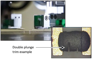
그림 3: 플라잉 프로브 접촉기가 장착된 레이저 트림 시스템. (출처: PPI 시스템즈)
Figure 3: Laser trim system equipped with flying probe contactors. (Source: PPI Systems)
자동화된 교정 루틴은 15 미크론 이내의 커팅 배치 정확도를 보장합니다. 커팅 너비는 일반적으로 10-50 미크론 범위입니다. 후막 저항기 기술을 고려하는 사람들은 인쇄된 이미지가 목표 저항기 값 범위를 충족하도록하기 위해 공정에 정확한 이미징과 일관된 재질 밀도가 필요하다는 것을 이해해야 합니다. 또한 인쇄된 후막 저항기의 인쇄 및 경화 복잡성으로 인해 인쇄 기판 제작 업체는 단일 기판 레이어에 저항기 기본 값 재질을 하나만 적용하는 것을 선호합니다. 그러나 제조업자가 잉크젯 유형의 증착 공정을 사용할 수 있다면 단일 회로 층에 두 개 이상의 기본 값 저항성 잉크 화합물을 적용하는 데 더 큰 관용도를 갖게 됩니다. 후막 저항기 형성 공정은 오랜 역사를 가지고 있으며 임베디드를 위한 인기 있고 저렴한 솔루션으로 남아 있지만 많은 PCB 제조 회사에서 이 기능을 제공하지 않을 수 있습니다. 후막 저항기 형성은 통제된 저장, 신중한 혼합, 인쇄 및 경화 작업이 필요한 습식 공정으로 간주되기 때문입니다. 임베디드 저항 기능을 제공하는 PCB 제조업체는 대체 박막 처리 솔루션을 선호하는 경우가 많습니다.
Automated calibration routines ensure cut placement accuracy within 15 microns. Cut widths are typically in the 10–50-micron range. Those considering thick-film resistor technology must understand that the process requires precise imaging and consistent material density to ensure that the printed image will meet the target resistor value range. And due to the printing and curing complexity for printed thick-film resistors, the printed board fabricator will prefer applying only one resistor base value material onto a single substrate layer. If the fabricator can use an inkjet-type of deposition process, however, they will have greater latitude in applying two or more base value resistive ink compounds onto a single circuit layer. Although the thick-film resistor forming process has a long history and remains a popular, low-cost solution for embedding, many PCB fabrication companies may not offer this capability. This is because thick-film resistor forming is considered a wet process requiring controlled storing, careful mixing, printing and curing operations. PCB fabricators that do offer embedded resistor capability will often prefer to adopt alternative thin-film processing solutions.
2부에서는 형성된 박막 저항기를 내장하기 위한 재질, 설계 규칙 및 공정 매개 변수를 검토할 것입니다.
In Part 2, I will review the materials, design rules, and process parameters for embedding formed thin-film resistors.

Vern Solberg는 SMT 및 마이크로 일렉트로닉스 설계 및 제조 기술을 전문으로 하는 독립적인 기술 컨설턴트입니다.
Vern Solberg is an independent technical consultant, specializing in SMT and microelectronics design and manufacturing technology.
레이저 트리밍 시스템 장비 구매 관련, 문의사항은 아래 연락처로 연락 바랍니다.
드림포토닉스
수원시 영통구 신원로 88 (신동 486) 디지털엠파이어2빌딩 103동 610호 [16681]
Mobile: 010-8781-0630 email: cbpark36@gmail.com
'레이저기술자료' 카테고리의 다른 글
| 대형 스테인리스 패널 레이저 마킹 시스템 (0) | 2021.09.24 |
|---|---|
| 피코초 레이저 유리 가공 시스템 (0) | 2021.07.19 |
| 정밀 미세 가공을 위한 고출력 UV 레이저 시스템 (0) | 2021.03.05 |
| 펨토초 레이저 유리 커팅 방법 개선 (0) | 2020.05.28 |
| 초고속 레이저 드릴링 방법 (0) | 2020.05.06 |


